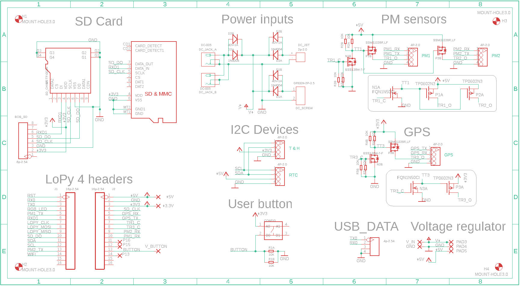
Circuit diagram
Many components appear to be duplicated on the schematic because they represent surface mount or through hole alternatives. (Indicated by A & B notation.) Be sure to only populate the one you need.
Pin assignment
Pin | Usage |
P0 | RX0 |
P1 | TX0 |
P2 | RGB LED |
P3 | PM1 TX |
P4 | RXD1 |
P5 | LOPY CLK |
P6 | LOPY MOSI |
P7 | LOPY MISO |
P8 | CS1 |
P9 | SDA |
P10 | SCL |
P11 | PM2 TX |
P12 | WIFI |
P13 | - |
P14 | BUTTON |
P15 | - |
P16 | - |
P17 | PM1 RX |
P18 | PM2 RX |
P19 | TR2 C |
P20 | TR1 C |
P21 | GPS TX |
P22 | GPS RX |
P23 | SD CLK |
P13, P15 & P16 are all input-only pins.
Last updated